Introduction
A USB audio DAC (Digital-to-Analog Converter) is an external device that converts digital audio signals from a computer or other USB-enabled device into analog audio signals that can be output to headphones, speakers, or other audio equipment.
The DAC is responsible for converting the digital audio signal (in the form of 1s and 0s) into an analog signal that can be sent to a headphone jack, speaker system, or other audio output.
Project Specs
- 2 x 15W Audio Output
- Supported for 8Ohm 20 W Speaker
- 15V Input Voltage
- Overcurrent protection
- Input supply reverse polarity protection
- USB to Analog audio bridge
- 3.5mm audio Socket for audio input/output
- Speaker overcuurent and short circuit protection
- Volume control- Mute/Up/down
- No Windows/Mac OS driver required
- Custom Audio output device name
Project Details
Audio DAC
In this project, I have designed a USB Audio DAC with 15W class D amplifier. Texas Instrument PCM2704C is used for the USB to Analog audio conversion. It is a single chip USB stereo audio DAC with USB 2.0 compliant full-speed protocol controller. This DAC does not need any driver installation in Windows/Mac/Linux machine. All the drivers are preinstalled by the TI in most of the OS.
We can change the name of the audio device that shows in the Windows audio output device list by our product name. when we plug the device then it shows the product name in the sound output setting of the Windows.

We can also increaser/decrease/mute the volume of the Windows using the DAC without any need of additional Windows/Mac driver.
Amplifier
Here, I have used MPS Class D amplifier MP7758. It is a 15W stereo output amplifier that can drive 8Ohm speakers.
Schematic
For Schematic and Layout (PCB) designing Altium CAD tool is used.
Schematic Block
1. Reverse Polarity Protection

This Block protects the circuit from the reverse connection of the input supply. information about the reverse polarity protection is mentioned here. A PMOS NVMFS5A140 is used here becurse it has very low Rds (4.2mΩ) so the voltage drop will be less at high current and power loss will be less. You can choose another PMOS here as per the component availability.
A 3A resetabble fuse/polyfuse (F1) is used to protect the circuit from overcurrnet protection. Any fault in the buck/DAC/amplifier cause excessive current flow that can damage the circuit. When the current goes beyond the fuse trip current then the fuse increases its resistance so that it can stop the current flow. The fuse is selected as per the Hold Current, Trip Current and Max voltage requirement. Here we need the hold current of 3A so it will trip on ~5A current. We can select the fuse as per our need from digikey like websites.
D2 is a TVS diode that used to suppress the ESD spikes. SZ1SMB30CAT3G is rated at 30V so it can used for max 30V input voltage. diode has clamping voltage of 48.4V so any voltage beyond this will be clamped by the diode. You can check the working of TVS diode here.
2. Buck Converter

A buck converter is used to convert the 15V to 3V3. The 3V3 is needed for the DAC (PCM2704C). A buck converter is better choice than LDO becurse the input voltage is high. If we used LDO then it has to drop 15V-3.3V=11.7V. So lets assume at 200mA current power loss will be 11.7 x 0.2A = 2.34 Watt in the from of heat.
A SY8113 buck regulator is used here . There are multiple buck regulators options availbe like TI,ST brand but the SY8113 is a cheap one in small package. You can choose another buck IC if this is not available (Need to change the buck schematic as per the IC). The output voltage of the buck can be set using the R2 & R4 resistor values. The datasheet mention the formula to calculate the values of the resistor.
R2 = (0.6 / (Vout - 0.6)) * R4.
So if we use R2=100K & Vout=3.3V then R4 = 22.1K
3. Audio DAC
The PCM2704C DAC has the USB input and analog audio output. A micro B USB connector (J2) is used to connect with the USB upstream port. TI provides the PCM2704C Evaluation module to test the IC before we use in the actual product. I have referred to the EVM schematic to design the circuit.
An EEPROM (IC2) is connected to the PCM2704C which used to store all the device descriptor information. The information contains the USB vendor Id, device ID, product string, vendor string. It is used to change the device name that shows in the windows audio output list. Only 8 bit EEPROM is supported by PCM2704C like AT24C16. It is a 16KB EEPROM (Internally Organized as 2,048 x 8 = 16Kb). I found that many other EEROM does not work with this DAC IC but AT24CXX series EEPROM works properly. The EEPOM has to be programmed before the assembly of the PCB. If the EEPROM not used/programmed properly then the default device name will be shown as “USB Audio DAC”.
The process of creating EEPROM hex file and programming is explained here
If we wanted to use external audio input (From 3.5mm audio connector J5) for the amplifier then DNP(do not populate) the R28 & R29 resistor. This will disconnect the Audio DAC from the amplifier. If we R28 & R29 is populateed then then audio connector J5 can be used as DAC output.
4. Amplifier The MP7758 is a dual output 15W amplifier. The amplifier is connected to the DAC output. The enable pin of the amplifier is connected to the DAC suspend pin so when no audio data comes from the host computer then DAC pull down the enable pin and disable the amplifier.
The switching of class D amplifier can create the EMI. To minimize the EMI a filter circuit is designed using the ferrit bead and capacitor.
The application circuit is referred from the datasheet to design this circuit.
Layout (PCB)
A four layer PCB is used for this project. As per the USB2.0 specs the USB D+/D- lines should be differential with 90 ohm impedance. So the Impedance controlled PCB is required. To achieve the 90Ohm trace impedance,we have to route the trace with specific trace width and trace clearance. This values can be provided by the PCB vendors as per the layer stackup or we can calculate it using the Saturn PCB toolkit. Layer 2 is used as ground reference plane for the D+/D- trace.
while layouting the Amplifier, DAC and buck converter, we have to follow design guideline provided by the company. In the datasheet of the IC we will get the design guideline. Below are the screenshot of the design guidline for the same.


PCB Layout


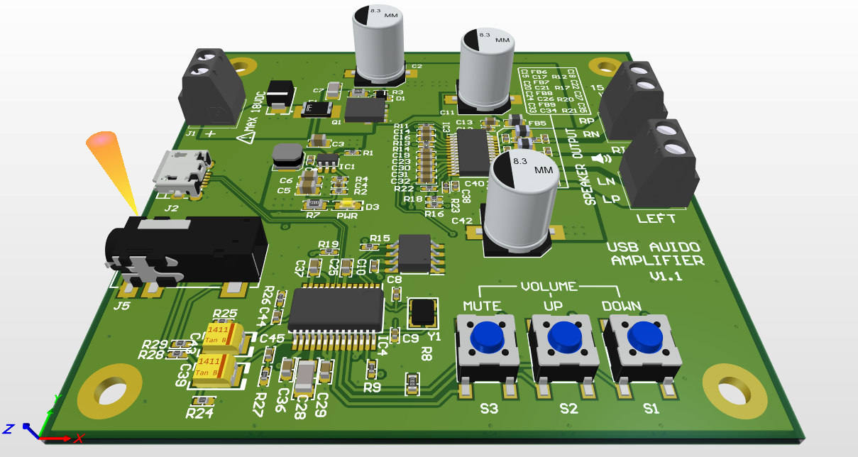
PCB Rendered Photo


PCB Specification
- PCB: 4 LAYER FR4
- THICKNESS :1.6mm
- COPPPER: 1 OZ EXTERNAL LAYER, 1 0Z INTERNAL LAYER
- SILKSCREEN: WHITE
- SOLDER MASK BOTH SIDE
- SOLDER MASK COLOR: BLACK
- ELECTRICAL BARE BOARD TEST REQUIRED
- IMPEDANCE CONTROL REQUIRED
- FINISH: LEADFREE HASL (/blog/usb-audio-amplifier/USB Audio DAC V1.1 Production Files.zip) USB_Audio_DAC_V1.1_Production Files.zip